The OrCAD design suite produced by the EMA Design Automation company is a powerful tool for anyone wishing to design a printed circuit board, or PCB. OrCAD's ultimate aim is to generate a Gerber file from a PCB schematic. A Gerber file contains all the necessary information for PCB manufacturing at a machining shop. To produce the Gerber file, you must generate a schematic, lay out a PCB and then route the PCB's tracks.
Click the "Capture" menu to begin generating your PCB design. Complete your basic PCB schematic with the drafting tools available.
Access the "Project" menu inside of the Project frame. Activate the Design Rules Check feature. OrCAD will check your design to make sure it is electronically functional. Correct any errors.
Open the "Project" menu again. Click "Create New Netlist," "Generate Netlist." Select the desired units, either metric or imperial.
Open and run the Layout Plus feature. Click "File," "New." Select a technology file that is suitable for your design. Technology files should be found in the Files\Layout_Plus\data folder. The easiest technology file to work with is the 1BET_ANY.TCH file because it allows for single tracks between pins.
Open the netlist file. The netlist file has an extension of .mnl. Opening the file should transfer all the footprints from the schematic over to the PCB layout window.
Draw the board outline by clicking on the "Obstacle" button on the toolbar. Right-click in the design window and select "Properties." Change the board's width and number of layers if desired. Drag and drop the electronic components by selecting the Components feature, which is located inside of the toolbar.
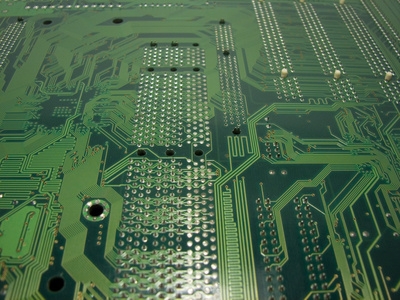
Route the PCB by automatically clicking "Tools," "Auto," "Route Board." You can use the "Unroute Board" option to undo any routing errors.
Generate the Gerber files by clicking "Auto," "Post Process." Now your PCB files are ready to be sent off to a manufacturing shop.